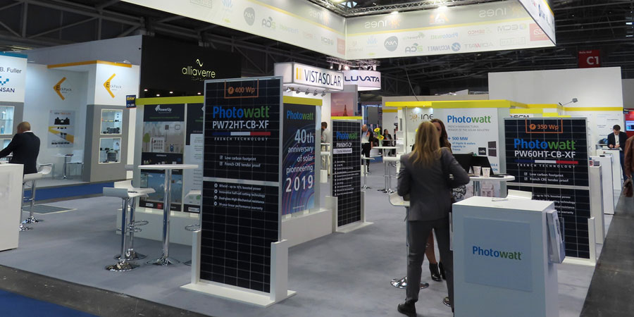
Photowatt participates in partnership with INES (National Institute for Solar Energy) in the INTERSOLAR exhibition in Munich. A collective 200m² stand shared with its industrial partners, experts and representatives of French know-how in solar energy, which aims to showcase the French solar sector.
Our team of experts awaits you for the next edition of Intersolar in 2021!
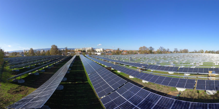
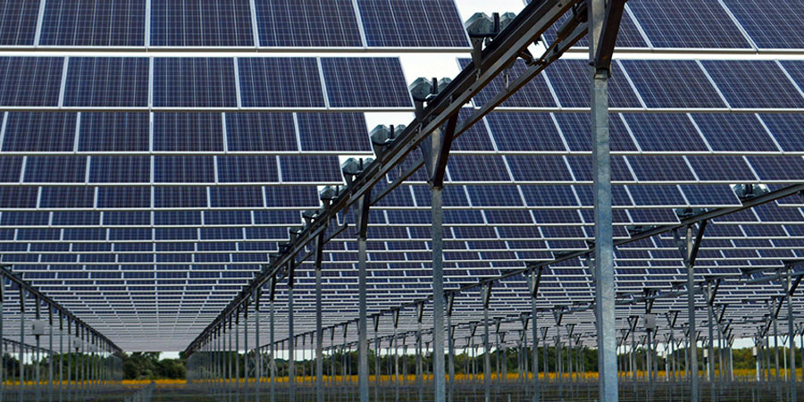
Produced in partnership with EGREGA and our low carbon modules. With an installed capacity of 5 MWp, it will produce 7 GWh / year, which is the equivalent of the electricity consumption of around 2,900 inhabitants!
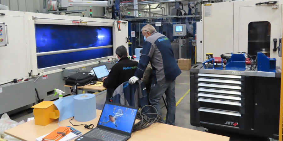
In partnership with GAOCE, in 2021 we finalized the installation of the new brick maker in our Bourgoin-Jallieu plant, which will allow us to offer you the new generation of larger, more efficient and low-carbon photovoltaic modules.
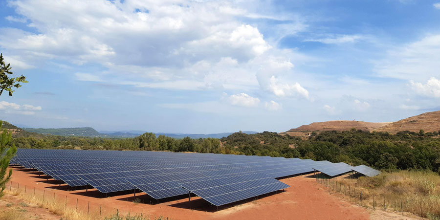
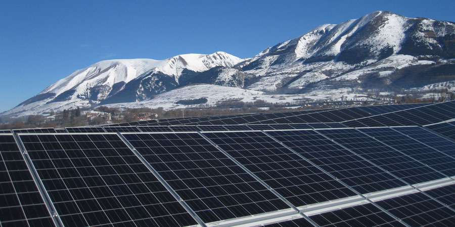
With a total capacity of 2.6 MW, the Le Luc photovoltaic power plant will produce 3,757 MWh of electricity per year, equivalent to the annual consumption of 1,830 people. In addition to its contribution to the ecological transition, the park participates in the revalorization of degraded land.
Photowatt places the environmental requirement in its priorities to make its activity and its practices consistent, whether it is to limit the carbon footprint, to organize the recycling of photovoltaic panels, or to respect the best standards of the profession. .
Photowatt photovoltaic modules generate 3 times less carbon than Asian modules and they are close to the ratios of thin film modules.
Based on ISO 9001 and ISO 14001 certifications as well as the most demanding product certifications in the profession, Photowatt places customer satisfaction at the heart of its priorities.
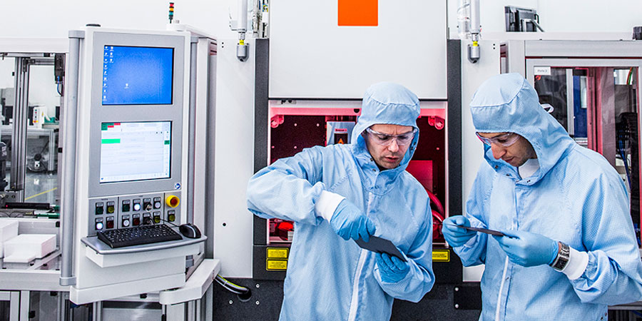
Continuous improvement in the manufacture of photovoltaic panels
At each stage of production, the company introduces process optimizations with a dual objective: lower production costs and increasing quality. With this scientific and technical capital, the mission of our team dedicated to R&D revolves around 2 main axes: accelerating the incorporation of incremental innovations into the manufacturing process and anticipating breakthrough innovations.
With its facilities and its ability to develop new processes, Photowatt focuses its research and development activities in conjunction with the R&D of the EDF group and research centers such as INES and the Photovoltaic Institute of Ile de France. in order to promote the emergence of new technological solutions for photovoltaic cells and modules.
Photowatt’s expertise as well as the technology and industrial capacity of its historical partners have enabled the company to seize the opportunities of a rapidly growing solar energy market.
Wafers, produced with a low carbon footprint, are today marketed in the form of photovoltaic modules within the framework of calls for tenders launched by the French Government in its Pluriannual Energy Programming (PPE) aimed at deploying around 2.5 GWp per year from photovoltaic projects.
The company’s transformation plan is based on mono-like “Crystal Advanced” technology, developed by INES and ECM, a global specialist in crystallization furnaces. Mono-like is an innovative technology in the crystallization of polycrystalline silicon which increases the yield of ingots and wafers to compete with PERC technology on monocrystalline wafers.
Share this page
Manage cookie consent
We use cookies to optimize our website and our service and you can modify your consent at any time on the page Cookie Policy.
Functionnal
Always active
The storage or technical access is strictly necessary for the purpose of legitimate interest to allow the use of a specific service explicitly requested by the subscriber or user, or for the sole purpose of carrying out the transmission of communication over an electronic communications network.
Preferences
Storage or technical access is necessary for the purpose of legitimate interest to store preferences that are not requested by the subscriber or user.
Statistics
Storage or technical access that is used exclusively for statistical purposes. List of partners: Matomo Analytics, ElementorStorage or technical access that is used exclusively for anonymous statistical purposes. Absent a subpoena, voluntary compliance from your internet service provider, or additional third party records, information stored or retrieved for this sole purpose cannot generally not be used to identify you.
Marketing
The storage or technical access is necessary to create user profiles in order to send advertisements, or to follow the user on a website or on several websites with similar marketing purposes. Third-party: LinkedIn.